Inside Intel’s Fab 52 — the Arizona mega foundry building the future of 2nm chips
From billion‑dollar construction feats to cutting‑edge RibbonFET and PowerVia tech, this is where Intel’s next‑gen processors are born.
Intel maintains a sizable presence in the United States, especially in Oregon and Arizona. I travelled to the latter for Intel Tech Tour 2025, where Intel shared a bevy of announcements near its absolutely massive Ocotillo campus.
I was able to take a tour of this campus, and most notably Fab 52 — the latest (and largest) addition packed with the most cutting-edge semiconductor fabrication technology in the world. It's this foundry that will produce Intel's next-gen processors using the new 18A processing node.
2026 could be a big year for Intel if its ambitions with Fab 52 are realized. Here's what you should know about Intel 18A, and I'll also share my experience strolling through the impressive Fab 52.
Article continues belowThe heart of Intel Panther Lake is 18A
I've spent some time breaking down Intel's next-gen Panther Lake mobile chips, and explained what you need to know about the new Intel Arc graphics being paired with them. I skimmed over Intel 18A, though, and why exactly it's important.
If you weren't aware, one of the most important metrics for gauging the progression of semiconductor fabrication is the size of individual transistors, measured in nanometers. The smaller the size, the more densely you can pack transistors. The more densely you can pack transistors, the more transistors you can have. The more transistors you can have, the better your chip's performance and efficiency (largely speaking).
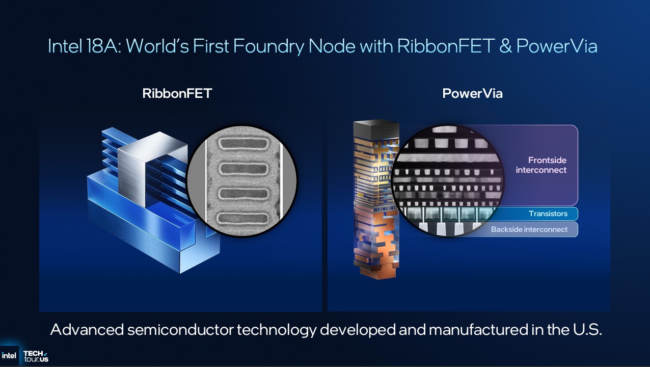
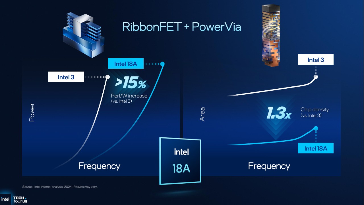
Intel 18A is a 2nm-class processing node, which is on the cutting edge of what modern semiconductor fabrication can achieve. That's important, but Intel 18A is special because it finally debuts two unique technologies in chips that are actually going to reach consumers — RibbonFET and PowerVia.
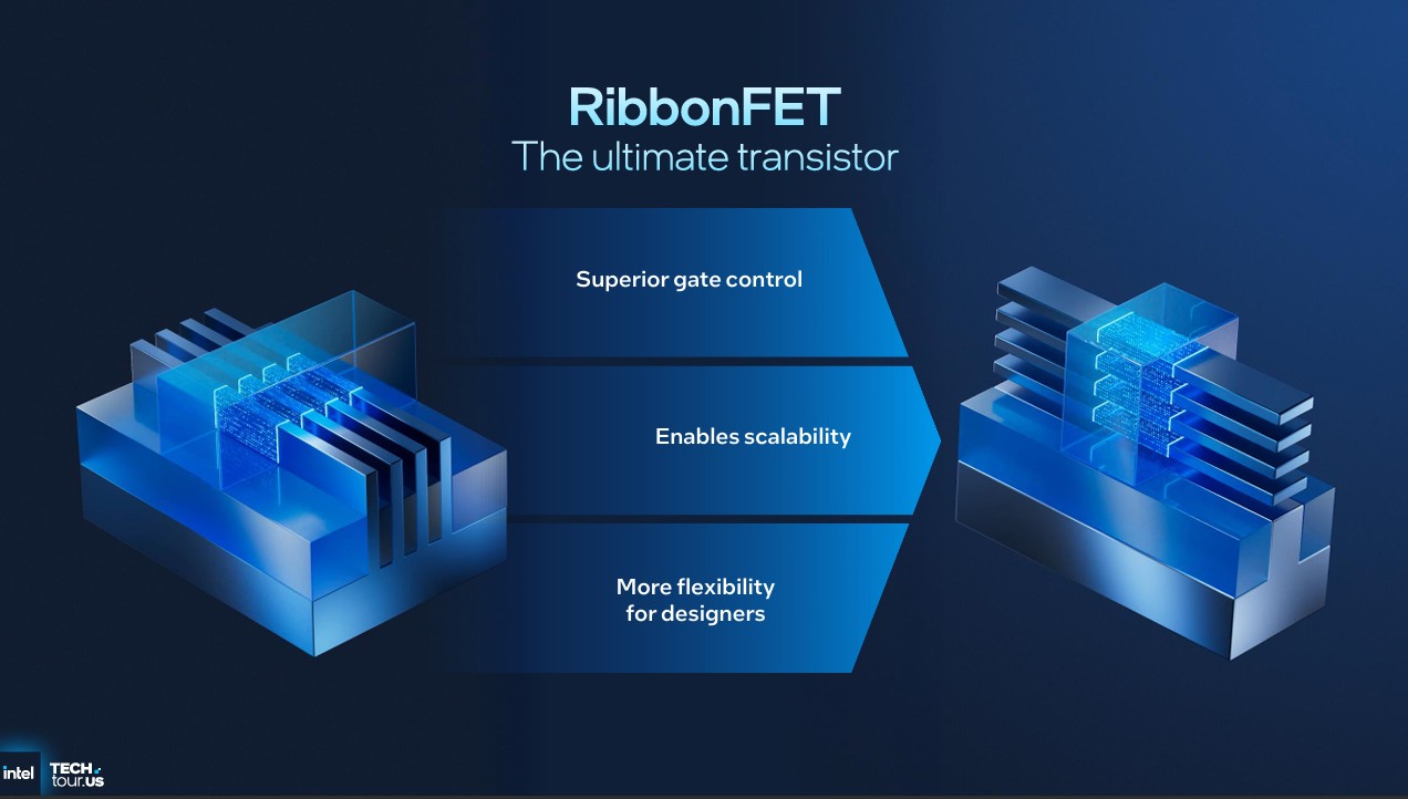
First, RibbonFET is set to replace the "FinFET" transistor design that has been the standard for over a decade. While the latter uses vertical "fin" transistors with the gate (which controls the flow of electricity through the transistors) set on top, RibbonFET uses a new, flexible and scalable "ribbon" design with a gate that wraps completely around the transistors. This design allows for more precise control, less power leakage, superior performance-per-watt, and helps support more densely packed transistors.
All the latest news, reviews, and guides for Windows and Xbox diehards.
RibbonFET and PowerVia aren't normal "year-over-year" improvements — they're fundamental changes to how processors are made.
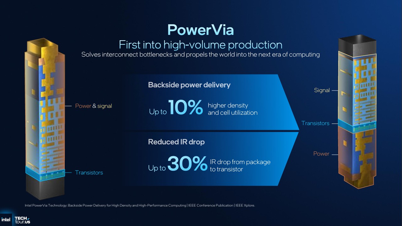
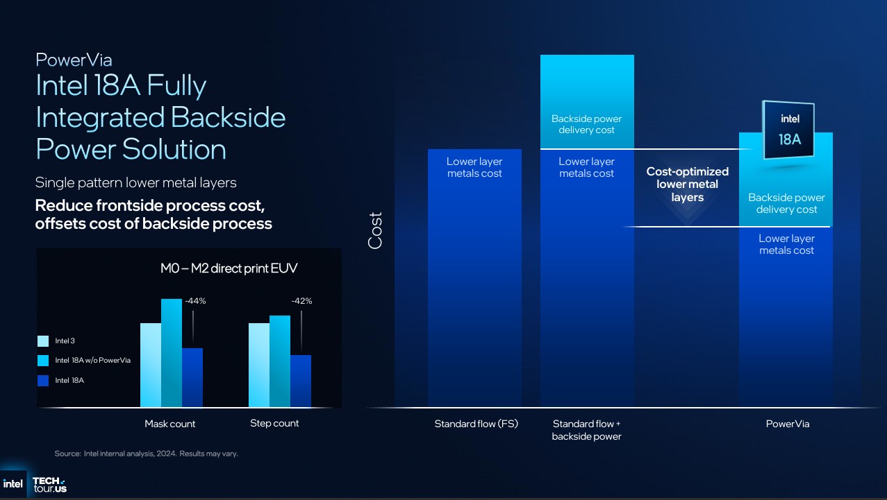
PowerVia is a similarly crucial advancement. Traditional chips weave together signal and power routing for transistors through the front of the chip die, but this can lead to congestion and performance degradation as transistors become more densely packed. With Intel 18A, chips can now route power to transistors through the backside of the die, leaving the front reserved just for signal input/output.
The result of these two technologies is significantly improved performance, efficiency, and consistency with intense, high-power workloads (like artificial intelligence). Intel 18A can also be paired with other Intel processing nodes thanks to Intel's more modular Foveros-3D advanced packaging, which can stack multiple, separate chiplets on the same die.
Intel Panther Lake is the first platform to be built using Intel 18A, and takes full advantage of these upgrades. As production scales up, too, we could see other partners turn to Intel for their semiconductor needs — and it's all happening inside Fab 52.
Fab 52 is alive, and I went aside to see what it's all about

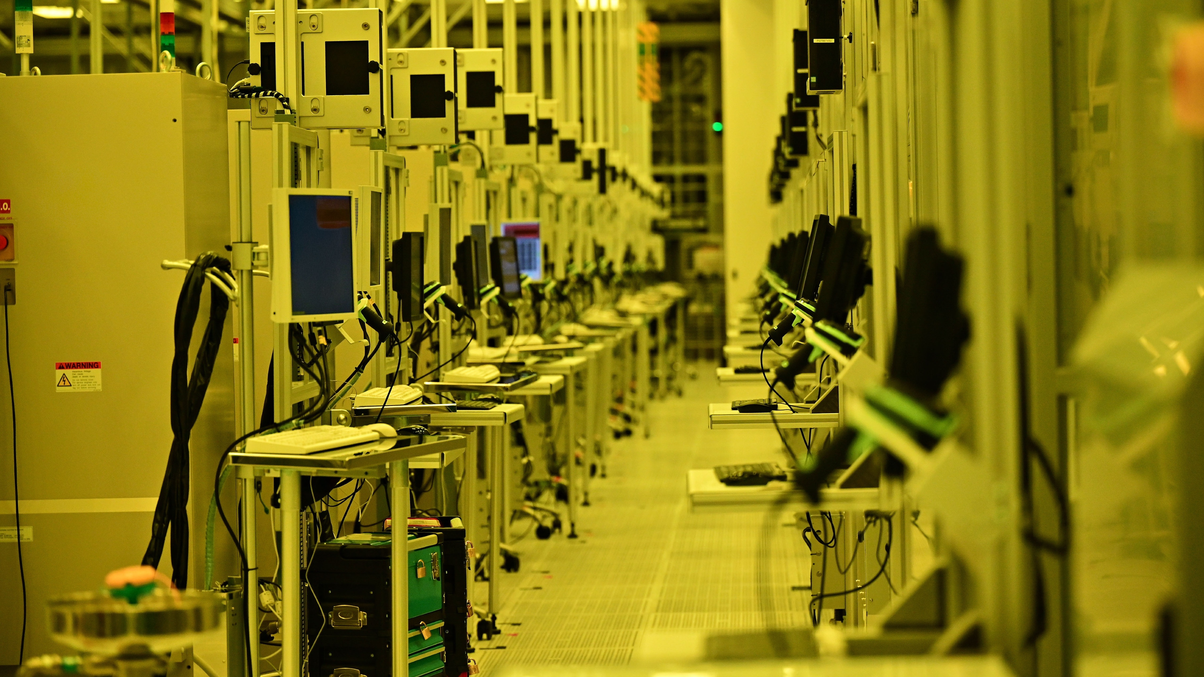
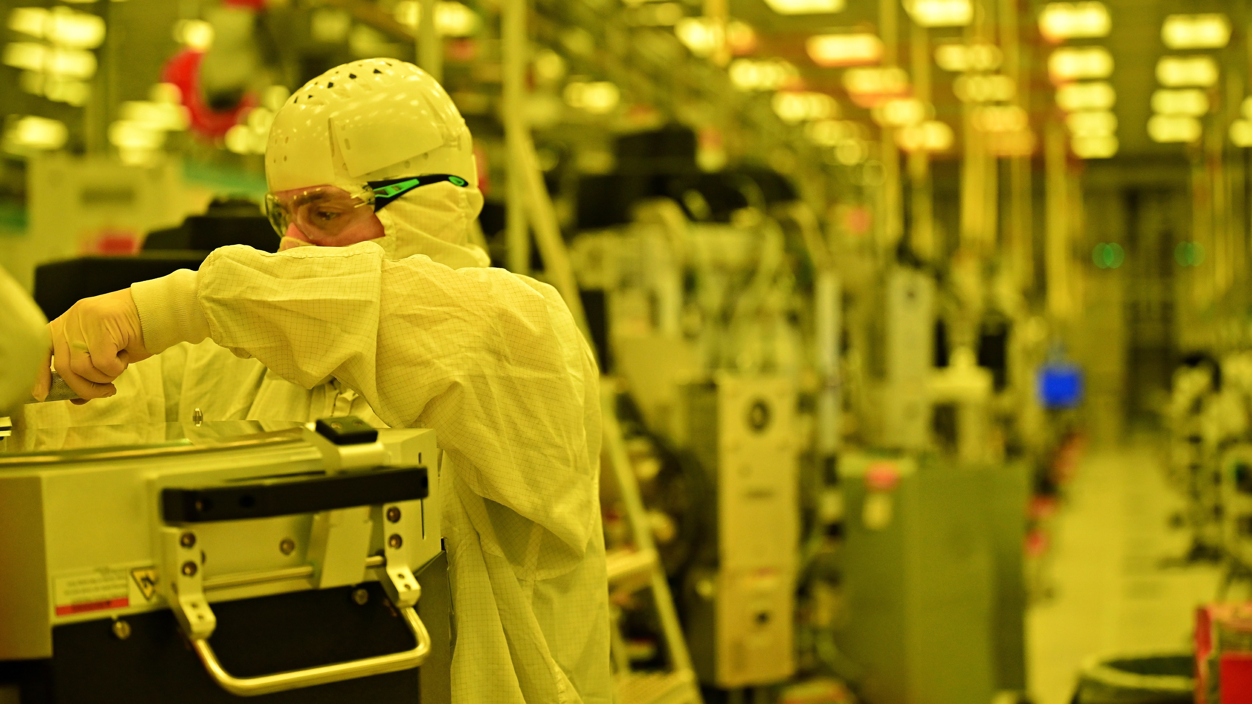
Intel's Ocotillo campus is massive. Constantly growing since it first opened in the 1990s, this campus is built on over a square mile of land with its own 12-acre water treatment and recycling plant, and Fab 52 — the latest addition — is large even by Ocotillo standards.
Four years of construction required thousands of workers and tens of billions of dollars of investment. Intel had to excavate the equivalent of over 400 Olympic pools filled with soil and rock, and poured over 600,00 cubic meters of concrete — so much concrete that Intel built its own mixing plant on-site — reinforced by over 75,000 tons of steel.
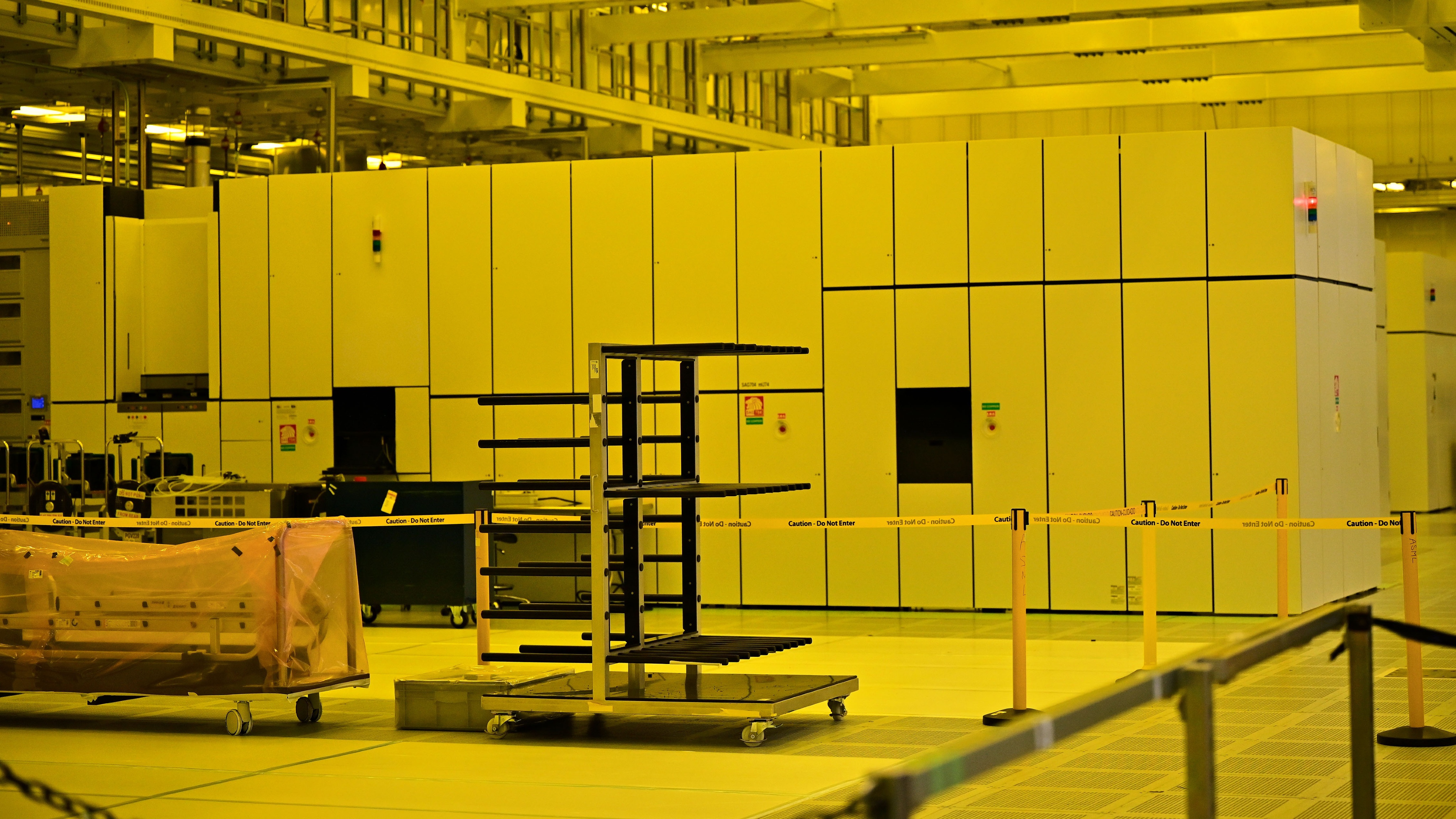
It wasn't just about erecting the largest building possible; Intel had to carefully plan how and where to reinforce the ground to support the impossibly heavy Extreme Ultraviolet Lithography (EUV) machines that are crucial for Intel 18A. These machines are so heavy it apparently takes three Boeing 747 cargo planes to transport just one to Arizona, and Fab 52 uses moveable bridge cranes built into its ceiling for construction and maintenance.
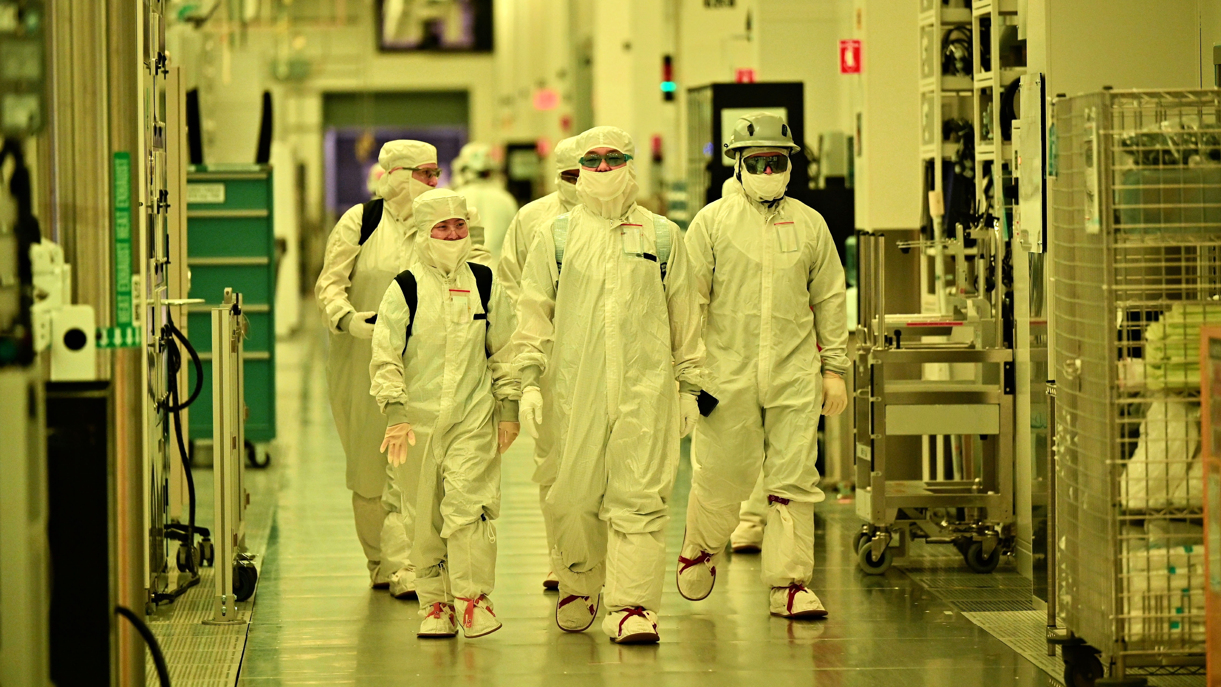
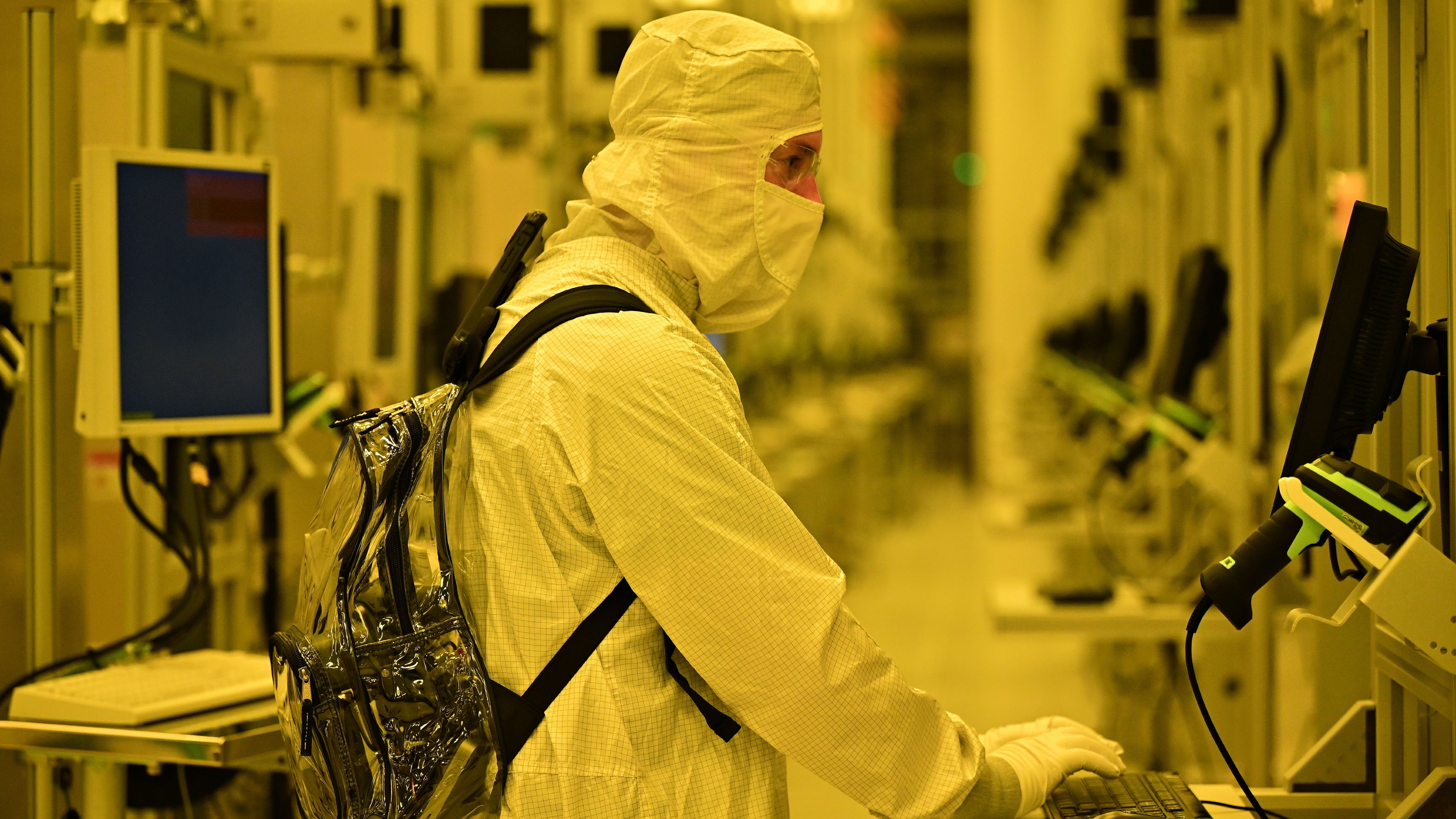
I got to see these EUVs in person, but I couldn't just stroll in. I had to leave my phone and all electronics behind (not just for Intel's security, but also because any wireless signal can interfere with the absurdly precise and delicate tools inside the foundry), and I had to don a hair net, gloves, and shoe covers before I was even allowed to enter the clean room where I was properly gowned in a full-body suit, hood, boots, protective goggles, and a second pair of gloves.
The best of engineering, chemistry, and material sciences, plus absurd levels of foresight, make semiconductor fabrication possible.
Enter the foundry, and you may note the aggressively "average" feeling of the air, as Intel carefully manages the temperature, humidity, and even air mixture. Dedicated air extraction towers cycle the air in the foundry six times a minute, apparently, and the air is thousands of times cleaner than even your average surgery operating room. You may also note the strange, yellow-green hue of the lighting, which is apparently an additional precaution to protect Intel's chips from the effects of some spectrums of light (similar to a dark room for developing older film).
I remember being mesmerized by the literal miles of track suspended from the ceiling, on which hundreds of automated robots carry silicon wafers and dies from tool to tool and building to building, the rows of extraordinarily advanced equipment, and the knowledge that the foundry is constantly under construction inside and out. Intel carefully considers which tools to replace or upgrade on a daily basis, ensuring that every foundry and building plays a role.
I won't even pretend to fully understand how exactly humanity managed to make rocks think, but I did learn a lot about semiconductor fabrication during my time with Intel in Arizona. I'm excited to see just how good Panther Lake ends up being, and it'll be especially interesting now that I've seen where Panther Lake chips are born.

Follow Windows Central on Google News to keep our latest news, insights, and features at the top of your feeds!

Zachary Boddy (They / Them) is a Staff Writer for Windows Central, primarily focused on covering the latest news in tech and gaming, the best Xbox and PC games, and the most interesting Windows and Xbox hardware. They have been gaming and writing for most of their life starting with the original Xbox, and started out as a freelancer for Windows Central and its sister sites in 2019. Now a full-fledged Staff Writer, Zachary has expanded from only writing about all things Minecraft to covering practically everything on which Windows Central is an expert, especially when it comes to Microsoft.
You must confirm your public display name before commenting
Please logout and then login again, you will then be prompted to enter your display name.

 Windows Central Insider


